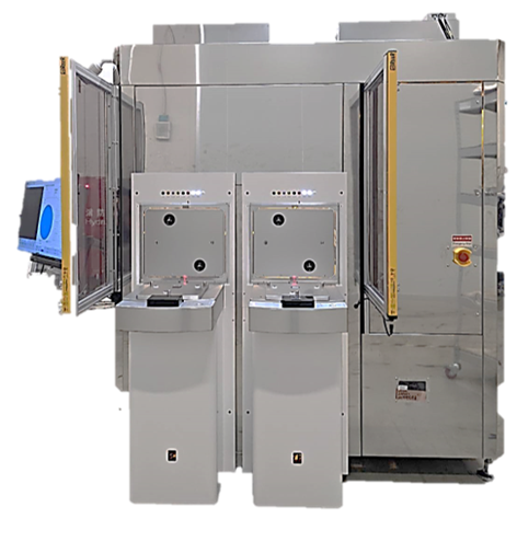
V5200/V5300 Pro
The world’s first automatic optical microscope inspection equipment V5200/V5300 Pro offers fully automatic macroscopic and microscopic inspection and measurement, satisfy wafer front-side and back-side inspection, and no longer traditionally manual operation with identification through human eyes. V5 has been certified by a number of advanced OSAT packaging plants. Our system supports online ASI, ACI, ADI, AEI, APDI, API, and ASTI testing and measurement and offline analysis.
Equipment capability
- It is used to inspect “8 and 12” (200mm/300mm) wafers.
- Wafer warpage handling capability is +/-7mm.
- Macro inspection “zero” blind spot to detect defects on the front-side and back-side of wafer.
- Microscopic inspection offers multiple magnifications. 6 magnifications are available: 2X, 5X, 10X, 20X, 50X and 100X, with resolution range 0.055um ~ 2.75um.
- Bump CD/line width/overlap/EBR/WEE measurement stability is within 1 pixel deviation.
- Multi-function settings to meet all quality assurance specifications.
- Online and offline software review
- The inspection results output in KLARF or SINF files according to specifications, including the coordinate information of the front-side of the wafer corresponding to the back-side defects.
- FAB automation support (OHT + SECS/GEM)
- Intelligent AI ADC software